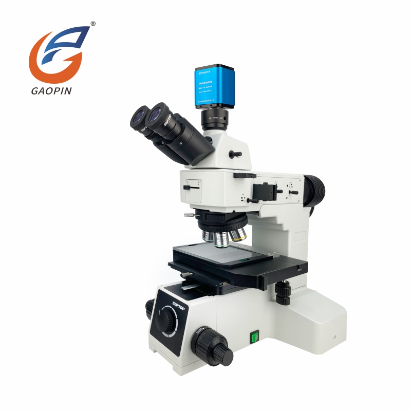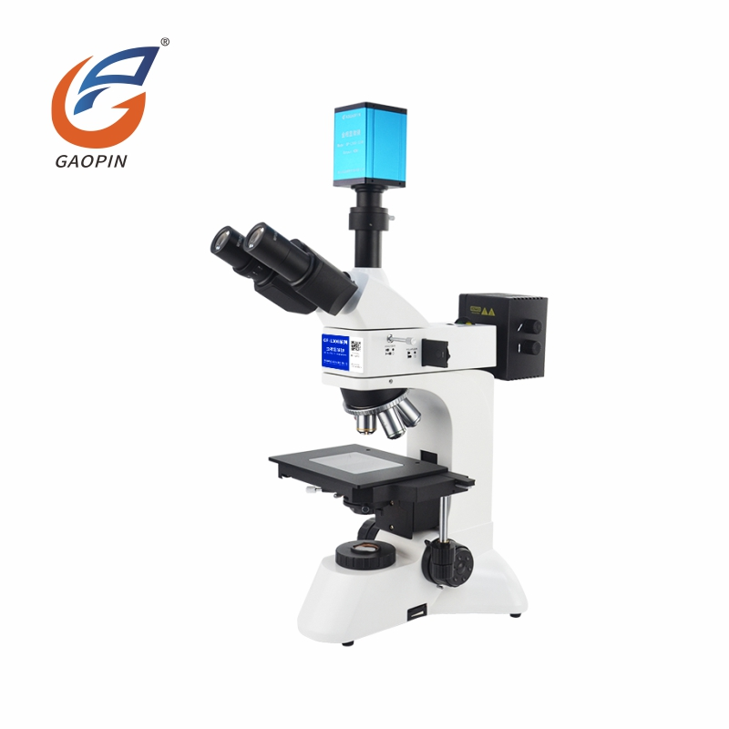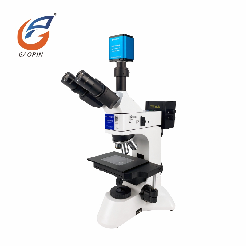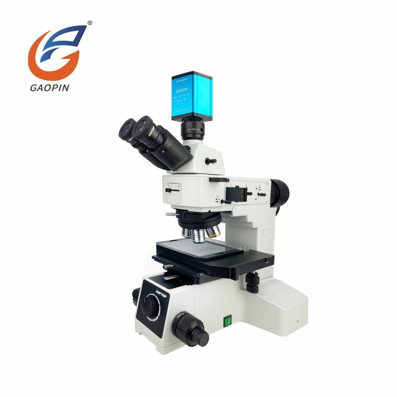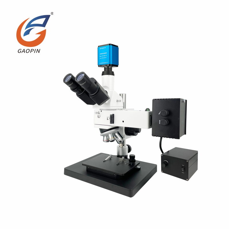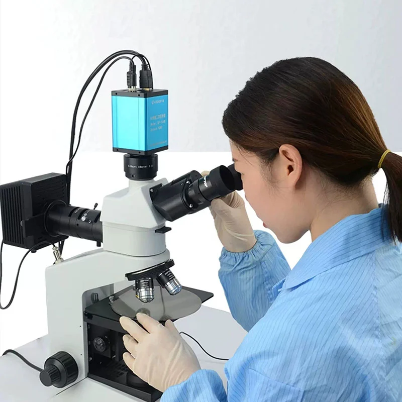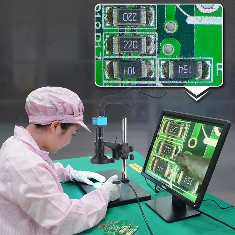
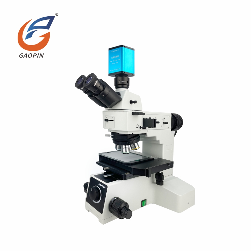
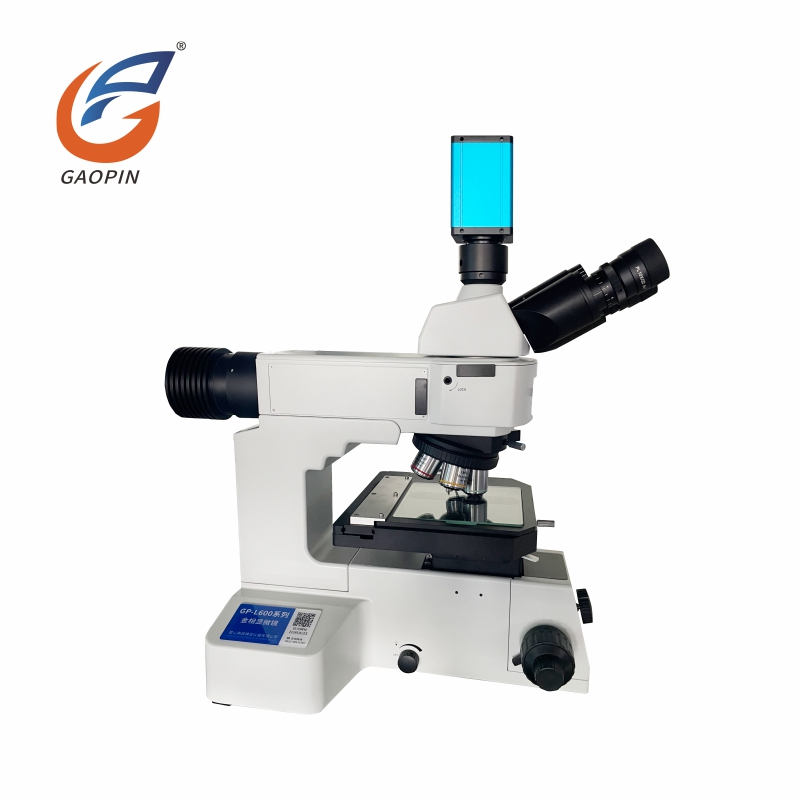
GP-L600-300C Metallurgical Microscope for Wafer Inspection is a Wafer Inspection Metallurgical Microscope specially designed for material-microstructure inspection. Equipped with high-resolution reflected-light optical system and DIC differential-interference function, it generates stereo-relief images for observing grain structures, cracks, inclusions and coating layers of metals, alloys, semiconductors and other materials. With industrial camera built-in, it supports image capture and on-monitor measurement; grain-size evaluation is available with optional supporting software. Widely applied in quality-control, failure-analysis and material-science-research scenarios.
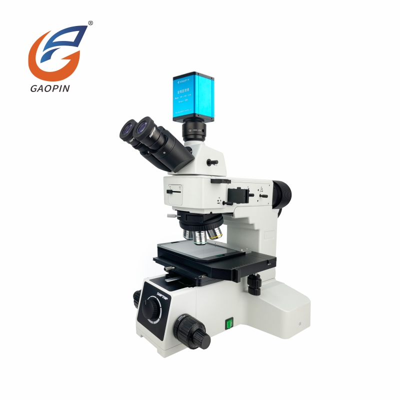
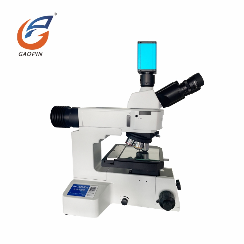
This Metallurgical Microscope for Wafer Inspection is suitable for microscopic observation of metallographic microstructures and surface morphology. It serves as an ideal research tool for metallurgy, mineralogy and precision-engineering disciplines.
1. Binocular viewing plus synchronous electronic observation: Eyepiece view and monitor display work synchronously. Ordinary metallurgical microscopes only support eyepiece observation; extra camera accessories are required for screen output.
2. High-precision mechanical body: Rigid mechanical structure with stable optical path, suitable for semiconductor and material-analysis work. Conventional metallurgical microscopes deliver lower mechanical precision.
3. Direct HDMI output: Real-time image output to monitor via HDMI cable. General metallurgical microscopes require separate cameras and capture cards for image output.
4. On-monitor offline measurement: Dimension measurement can be completed directly on-monitor without PC connection. Ordinary metallurgical microscopes rely exclusively on PC-software measurement.
5. Offline U-disk storage: Save photos and videos onto U-disk without a computer. Traditional models must connect to PC for image saving.
6. Dedicated metallurgical optical path: Optimized for metal-grain, coating, semiconductor and metallographic inspection. Ordinary digital microscopes lack this specialized optical path and cannot visualize metallographic structures.
HD camera built-into trinocular housing for simultaneous viewing via eyepiece and monitor. HDMI real-time micro-image output combines observation and recording workflows.
Supports DIC, bright-field, dark-field and polarized-light observation. 4-step magnification, optical 50-500X, max digital magnification up to 1900X, delivering sharp details for micro-feature inspection.
Dual focus knobs paired with reinforced lens-barrel assembly enable steady focusing and minimize image shaking.
Thick integrated metal body and stage bracket with low center-of-gravity, keeping stable performance for long-duration laboratory observation.
Minimalist all-white rigid-metal structure with modular optical layout, well-suited for laboratories and research institutes.
Ideal for wafer inspection, metallographic analysis, material-microstructure characterization, academic-research and precision-quality-evaluation work.
1080P photo & video capture, built-in on-monitor measurement, U-disk storage. Digital images simplify file archiving, comparison and post-experiment analysis.
Mechanics: Full-metal construction for high rigidity and vibration resistance. Precision coarse-fine focusing without backlash. High-precision manual XY mechanical stage with low wear and minimal clearance. Trinocular optical path maintains optical co-alignment during magnification switching.
Optics: Infinity-corrected plan-achromatic metallurgical objectives with anti-fog hard coating. Transmitted-reflected 12V-100W halogen-lamp illumination.
Imaging and Measurement: Industrial-grade HDMI 1080P camera with excellent anti-interference performance, suitable for industrial-environment operation. Measurements are performed via firmware on the display.
Operating Environment: Working temperature 10-35℃, relative humidity 30-75%RH. Stable performance under regular factory electromagnetic-environment. Avoid heavy vibration, corrosive gas and heavy dust.
Quality & Maintenance: Full-item factory inspection. Do not disassemble optical modules. Regular dust-proof cleaning will extend service life.
Semiconductor & Microelectronics (Core DIC Application):
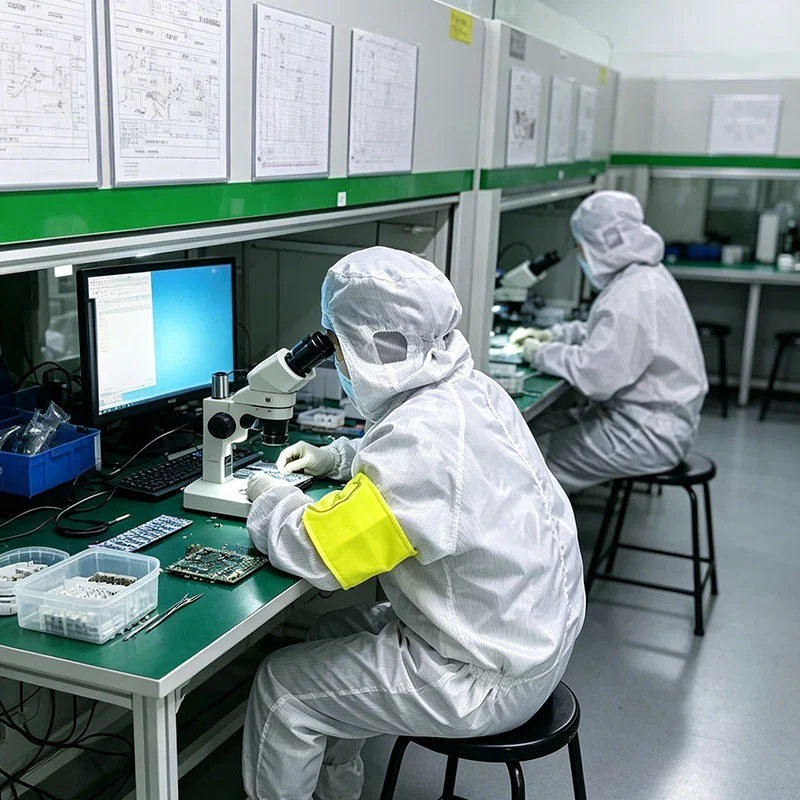
Silicon wafers, lithography slices, IC chips, PCBs, FPC flexible circuits, solder joints, packaging components.
Inspection targets: chip-surface topography, wafer-etching patterns, nano-scratches, cold-soldering joints,
oxidation and pin deformation. Differential-interference-contrast (DIC) highlights subtle surface height differences
for micro-circuit-slice observation within 190-1900× magnification range.
Metallographic Metal Specimens:
Alloy metallographic sections, steel, precision-stamped metal hardware.
Inspection targets: metal grain structure, heat-treatment analysis, micro surface cracks, edge chipping, fine burrs,
wear traces and internal material impurities. Bright-field / dark-field / polarized-light modes available for metal
crystal structure observation.
Lab Research Samples: Crystal, Powder, Fiber & Thin-Film:
Chemical crystals, metal powder, carbon fiber, textile fiber, optical-coating-films.
Observe crystal morphology, particle outlines, film delamination and micro-coating textures; polarized-light
identifies crystal-polarization characteristics.
Optoelectronic Precision-Plastic Components:
LED chips, optical lenses, glass substrates, semiconductor-packaging glue.
Detect micro-pores, nano-scratches, glue-delamination, bubbles and subtle surface unevenness.
High-Precision Miniature Components:
Connectors, terminals, micro-springs, tiny stamped-workpieces.
Pixel-level accurate measurement for gaps, hole diameters, pitch and surface-height-differences; DIC visualizes
subtle crimp-deformation.
University Labs & High-End Semiconductor QC:
Material-research experiments, wafer incoming-goods inspection, metallographic-specimen observation; photo-video
archiving.
Equipped with native 1920*1080 HD imaging. Suitable for metallographic observation, basic-semiconductor inspection and simple-laboratory-report generation; clearly displays metal grains and tiny circuit defects.
Manual-focus design, suited for static-laboratory samples and low-frequency workpiece-replacement. Stable focusing structure with precise fine-tuning for detailed static-sample observation.
Standard manual moving stage and vertical trinocular metallurgical optical-path for metal specimens, chip slices and medium-small-size PCBs, effectively suppressing reflective glare for basic metallographic-inspection.
Dual-magnification-range: 50-500X optical magnification, 190-1900X digital magnification. Covers both full-specimen overview and micro-grain / micro-defect inspection.
Built-in on-device measurement function, HDMI real-time output, U-disk for saving inspection photos and measurement data, for basic-laboratory-archiving purposes.
Neutral-packing shipment is available upon request.
| Item | Description |
| Product | GP-L600-300C Wafer Inspection Metallurgical Microscope |
| Category | Laboratory Research-Grade Trinocular Metallurgical Microscope, supports DIC differential-interference, bright-field / dark-field / polarized-light observation |
| Core Technologies | Trinocular synchronous-viewing optical system, multi-mode integrated illumination (bright-field, dark-field, polarizer, differential-interference-contrast DIC), professional high-precision metallurgical objective-lens set, HD CMOS imaging sensor, built-in digital-precision-measurement module, HDMI real-time-video output, U-disk local-image-storage technology |
| Key Specifications | Visual magnification: 50/100/200/500×; Electronic magnification: 190/380/760/1900×; Output interface: HDMI only; Capture resolution: 1920*1080; Manual-focus only; Built-in precise-measurement function; U-disk storage; Monitor-terminal supports HD-image preview, photo-capture and video-recording; Observation modes include differential-interference, bright-field, dark-field, polarized-light. |
| Typical Applications | Semiconductor-wafer-failure-analysis, metal-material metallographic-testing, coating-thin-film- microstructure-observation, precision-semiconductor-package-inspection, new-material-laboratory-research, medical-biomaterial-observation, micro-defect-detection for electronic-components |
| Manufacturer | Kunshan Gaopin Precision Instrument Co., Ltd. |
| Manufacturer Location | Kunshan, Jiangsu, China (adjacent to Shanghai) |
| Model | GP-L600-300C |
| Resolution | 1920×1080 |
| Real Effective Pixels | 2 Megapixels |
| Focusing Method | Manual focus only |
| Optical Format | 1/2" |
| Pixel Size | 3.75 μm × 3.75 μm |
| Output Method | HDMI |
| Detailed Introduction for Output Interfaces | ① HDMI connects to 4K-compatible displays. Embedded professional image-processing firmware supports photo-recording, video-recording, dimensional measurement, image playback and image comparison, operated by mouse in real-time. |
| Frame Rate | HDMI: 60fps @1920*1080 |
| Depth-of-Field Synthesis | / |
| Image Stitching | / |
| Measurement Method | Built-in on-monitor measurement system |
| Measurement Accuracy | 0.001 mm |
| Measurement Units | mm / μm / mil / inch (4 switchable units) |
| Measurement Tools | Length, angle, radian, circle, polygon, polyline, center-to-center distance, rectangle, annotation adding, automatic edge detection, scale bar and more |
| Storage Method | U-disk storage |
| Display Language | Simplified Chinese / English (switchable) |
| Processor | ARM Cortex-A7 Dual-Core @ Max 1.3 GHz |
| Operating System | Independently-developed measurement firmware based on Linux 3.1 kernel |
| Image Naming | Automatic or manual naming available |
| Viewing Head | 30°-inclined hinge-type trinocular head; inter-pupillary adjustment range: 54-76 mm; two beam-splitting ratios: 100:0, 0:100 |
| Observation Modes | ★ Bright-field / Dark-field / Polarized-light / DIC (DIC hardware is optional) |
| Illumination System | Transmitted-reflected falling-light illumination system, 100-240V wide-voltage input, adjustable filament center, continuously-adjustable light intensity. |
| Stand |
① Dual-purpose transmitted-reflected rack; low-hand-position coaxial coarse-fine focusing mechanism.
Coarse-adjustment stroke: 33 mm; fine-adjustment accuracy: 0.001 mm. Equipped with locking and limiting
devices ② Bright-field & dark-field reflector with variable aperture stop, field stop and adjustable-center assembly. ③ Interference filter and color-balance plate (white-light) for reflected-light optical path. ④ Light-dark-field switching device; slots for color filters and polarizing accessories. |
| Mechanical Stage | 4-inch manual mechanical stage. Stage dimension: 230 mm × 215 mm; X-Y travel: 105 mm × 105 mm. Glass specimen-carrier plate for both transmitted & reflected observation. |
| Light Source | 12V 100W halogen lamp chamber (reflected light); 12V 100W halogen lamp (transmitted light). |
| Polarization Function | 30-degree polarizer socket (reflected light); 360° rotatable analyzer socket for polarized-light observation. |
| Eyepieces | Two PL10X/22 mm wide-angle plan-field eyepieces with adjustable diopter (one eyepiece with reticle scale). |
| Nosepiece | ★ Bright-dark-field five-hole objective nosepiece |
| DIC Function | Differential-interference-contrast function; DIC insert-board accessories are optional and not included in standard configuration. |
| Electronic Interface | 0.5X C-mount camera interface, adjustable focus; CTV 1X is optional with price-difference compensation. |
| Metallurgical Objectives |
★ Bright-dark-field semi-destructive metallurgical objectives ① OLIPBD5NCA-DIC 5X/0.15, Working Distance: 9.00 mm ×1pc ② OLIPBD10NCA-DIC 10X/0.30, Working Distance: 9.00 mm ×1pc ③ OLIPBD20NCA-DIC 20X/0.45, Working Distance: 3.40 mm ×1pc ④ OLIPBD50NC 50X/0.55, Working Distance: 7.50 mm ×1pc ⑤ OLIPBD100NC 100X/0.80, Working Distance: 2.10 mm (optional, not included in standard package) |
| Optical Magnification | 50X, 100X, 200X, 500X (four-level switchable) |
| Electronic Magnification | Approx. 190X, 380X, 760X, 1900X (four-level switchable); optional magnification range: 380-3800X. |
Disclaimer: Logos and names of enterprises, universities and research-institutions appearing on this website only indicate that such entities have purchased or utilized GAOPIN-brand microscopes. Their appearance shall not be construed as purchase of this exact product model, and shall not imply any commercial endorsement, co-branding, affiliation or joint-project partnership with these third-party organizations.
GAOPIN microscopes are used by leading enterprises, research institutes, and universities. Our collaborative relationships include:
AVIC Optronics Technology Co., Ltd. – Precision-connector and component-inspection
NIO Shanghai – Precision-inspection for new-energy auto-parts & wiring-harnesses
Shanghai Institute of Ceramics, CAS – Micro-analysis of inorganic-ceramics & new-energy-materials
ZHENGKUNHANG Industrial MRO Supermarket (Shanghai) Co., Ltd. – Appearance & micro-quality-verification for industrial-standard-parts
Beijing Institute of Technology – Scientific-research-analysis for military-materials & optoelectronic-devices
GREE Electric Appliances (Hefei) – Precision dimension-measurement and defect-inspection for home-appliance-parts
Kunshan Gaopin Precision Instrument Co., Ltd. was officially founded in 2011. Our founder started research and manufacturing of optical-inspection-equipment as early as 2005 and accumulated abundant industry-experience. We deliver full-cycle-services covering product-design, technical-R&D, global-sales and comprehensive-after-sales-maintenance. Our in-house engineering team has over ten-years of experience in optical-system-development to ensure stable technical-performance and reliable-product-quality.
GAOPIN offers more than one-hundred categories of optical-inspection-instruments serving industrial-and-laboratory- clients worldwide. We provide flexible, cost-effective customized microscopy-solutions for diverse industrial quality-control and laboratory-analysis-projects.
For overseas-buyers, we provide timely global-technical-support including online-video-consultations, operational-video- tutorials and remote-skill-training. Our manufacturing-facility is located in Kunshan, Jiangsu Province (close to Shanghai). On-site-factory-visits and virtual-online-tours are welcomed. Please contact our sales-team for authentic sample-testing-images captured by this Wafer Inspection Metallurgical Microscope to evaluate real-imaging-performance.
A1: Only HDMI high-definition output is equipped. There is no USB, WIFI or LAN port. Computer connection is not supported; it works independently with a monitor for simple-operation workflows.
A2: Check power-supply and matching adapter; fasten HDMI cable firmly; switch monitor to correct HDMI signal source; restart device to resolve black-screen and no-image faults.
A3: This is a manual-focus model. Slowly adjust focus handwheel to obtain sharp imaging. Lock objective lens firmly, lay sample flat, and regularly clean lens dust and stains for clear view.
A4: Only FAT32-formatted U-disks ≤32 GB are supported. NTFS and exFAT formats are incompatible. Re-insert, re-format or replace with a compliant U-disk for normal photo and video saving.
Address
Building 2, Shuanglian International Business Center, Huaqiao Town, Kunshan City, China
Tel